

How Many Gated D-latches Are Present In 4 16-bit Registers?
![]()
An blithe interactive SR latch (R1, R2 = 1kΩ; R3, R4 = 10kΩ).
In electronics, a flip-flop or latch is a circuit that has two stable states and can be used to store state information – a bistable multivibrator. The circuit can be made to modify land by signals applied to one or more command inputs and will have ane or two outputs. It is the bones storage element in sequential logic. Flip-flops and latches are fundamental building blocks of digital electronics systems used in computers, communications, and many other types of systems.
Flip-flops and latches are used as data storage elements. A flip-flop is a device which stores a single bit (binary digit) of data; one of its ii states represents a "one" and the other represents a "zero". Such data storage can be used for storage of state, and such a excursion is described as sequential logic in electronics. When used in a finite-state machine, the output and next state depend not only on its electric current input, just besides on its current state (and hence, previous inputs). It can also exist used for counting of pulses, and for synchronizing variably-timed input signals to some reference timing betoken.
Flip-flops can be either level-triggered (asynchronous, transparent or opaque) or edge-triggered (synchronous, or clocked). The term flip-flop has historically referred generically to both level-triggered and edge-triggered circuits that store a unmarried fleck of data using gates. Recently, some authors reserve the term flip-flop exclusively for discussing clocked circuits; the simple ones are usually chosen transparent latches.[1] [two] Using this terminology, a level-sensitive flip-flop is called a transparent latch, whereas an edge-triggered flip-flop is simply chosen a flip-flop. Using either terminology, the term "flip-flop" refers to a device that stores a single scrap of data, only the term "latch" may also refer to a device that stores whatsoever number of bits of data using a single trigger. The terms "edge-triggered", and "level-triggered" may be used to avoid ambiguity.[3]
When a level-triggered latch is enabled it becomes transparent, but an edge-triggered flip-flop's output simply changes on a single blazon (positive going or negative going) of clock border.
History [edit]

Flip-bomb schematics from the Eccles and Hashemite kingdom of jordan patent filed 1918, one fatigued as a cascade of amplifiers with a positive feedback path, and the other as a symmetric cross-coupled pair
The first electronic flip-bomb was invented in 1918 past the British physicists William Eccles and F. W. Jordan.[four] [5] It was initially chosen the Eccles–Hashemite kingdom of jordan trigger circuit and consisted of two active elements (vacuum tubes).[6] The pattern was used in the 1943 British Colossus codebreaking computer[7] and such circuits and their transistorized versions were common in computers even after the introduction of integrated circuits, though flip-flops made from logic gates are also common now.[eight] [9] Early flip-flops were known variously as trigger circuits or multivibrators.
According to P. 50. Lindley, an engineer at the United states of america Jet Propulsion Laboratory, the flip-flop types detailed beneath (SR, D, T, JK) were get-go discussed in a 1954 UCLA course on computer design past Montgomery Phister, and and so appeared in his book Logical Blueprint of Digital Computers. [ten] [eleven] Lindley was at the fourth dimension working at Hughes Shipping under Eldred Nelson, who had coined the term JK for a flip-flop which changed states when both inputs were on (a logical "1"). The other names were coined by Phister. They differ slightly from some of the definitions given beneath. Lindley explains that he heard the story of the JK flip-bomb from Eldred Nelson, who is responsible for coining the term while working at Hughes Aircraft. Flip-flops in use at Hughes at the time were all of the type that came to exist known as J-G. In designing a logical system, Nelson assigned letters to flip-flop inputs as follows: #one: A & B, #two: C & D, #3: E & F, #4: G & H, #5: J & K. Nelson used the notations "j-input" and "yard-input" in a patent application filed in 1953.[12]
Implementation [edit]

Flip-flops can be either simple (transparent or asynchronous) or clocked (synchronous). In the context of hardware clarification languages, the uncomplicated ones are ordinarily described as latches,[1] while the clocked ones are described equally flip-flops.[2]
Elementary flip-flops tin can be built around a unmarried pair of cantankerous-coupled inverting elements: vacuum tubes, bipolar transistors, field effect transistors, inverters, and inverting logic gates accept all been used in practical circuits.
Clocked devices are specially designed for synchronous systems; such devices ignore their inputs except at the transition of a dedicated clock betoken (known as clocking, pulsing, or strobing). Clocking causes the flip-bomb either to alter or to retain its output signal based upon the values of the input signals at the transition. Some flip-flops alter output on the rising edge of the clock, others on the falling edge.
Since the simple amplifying stages are inverting, two stages tin can be connected in succession (equally a pour) to form the needed non-inverting amplifier. In this configuration, each amplifier may exist considered as an active inverting feedback network for the other inverting amplifier. Thus the ii stages are connected in a non-inverting loop although the circuit diagram is usually drawn as a symmetric cross-coupled pair (both the drawings are initially introduced in the Eccles–Jordan patent).
Flip-flop types [edit]
Flip-flops can be divided into mutual types: the SR ("gear up-reset"), D ("data" or "filibuster"[thirteen]), T ("toggle"), and JK. The behavior of a particular blazon tin can be described past what is termed the characteristic equation, which derives the "next" (i.e., after the next clock pulse) output, Q side by side in terms of the input signal(southward) and/or the current output, .

Simple fix-reset latches [edit]
When using static gates as building blocks, the near key latch is the elementary SR latch, where S and R stand for set and reset. Information technology can be constructed from a pair of cantankerous-coupled NOR or NAND logic gates. The stored bit is present on the output marked Q.
SR NOR latch [edit]
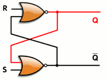
An animation of a SR latch, synthetic from a pair of cross-coupled NOR gates. Red and blackness mean logical '1' and '0', respectively.

An blithe SR latch. Black and white hateful logical '1' and '0', respectively.
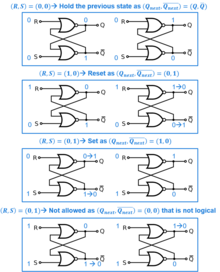
- S = one, R = 0: Set
- S = 0, R = 0: Concord
- S = 0, R = i: Reset
- S = one, R = 1: Not immune
Transitioning from the restricted combination (D) to (A) leads to an unstable state.
While the R and S inputs are both low, feedback maintains the Q and Q outputs in a abiding land, with Q the complement of Q. If S (Set) is pulsed high while R (Reset) is held low, then the Q output is forced loftier, and stays high when Southward returns to depression; similarly, if R is pulsed high while Southward is held depression, then the Q output is forced low, and stays low when R returns to low.
-
SR latch operation[iii] Feature table Excitation table S R Qnext Action Q Qadjacent S R 0 0 Q Agree country 0 0 0 X 0 1 0 Reset 0 1 1 0 ane 0 1 Set up 1 0 0 1 1 1 Ten Not allowed one ane 10 0
Notation: 10 ways don't care, that is, either 0 or 1 is a valid value.
The R = Southward = 1 combination is called a restricted combination or a forbidden state because, as both NOR gates then output zeros, it breaks the logical equation Q = not Q. The combination is likewise inappropriate in circuits where both inputs may go low simultaneously (i.east. a transition from restricted to go on). The output would lock at either 1 or 0 depending on the propagation time relations between the gates (a race condition).
How an SR NOR latch works.
To overcome the restricted combination, one can add gates to the inputs that would catechumen (S, R) = (one, i) to one of the non-restricted combinations. That tin can exist:
- Q = 1 (one, 0) – referred to as an South (dominated)-latch
- Q = 0 (0, 1) – referred to as an R (dominated)-latch
This is done in nearly every programmable logic controller.
- Proceed state (0, 0) – referred to as an East-latch
Alternatively, the restricted combination can be made to toggle the output. The upshot is the JK latch.
The characteristic equation for the SR latch is :
- or [14]


Another expression is :
- with [15]


SR NAND latch [edit]

An SR latch constructed from cantankerous-coupled NAND gates.
The circuit shown beneath is a basic NAND latch. The inputs are more often than not designated Due south and R for Set and Reset respectively. Because the NAND inputs must normally be logic ane to avert affecting the latching action, the inputs are considered to be inverted in this circuit (or active low).
The circuit uses feedback to "think" and retain its logical state even subsequently the controlling input signals have changed. When the Due south and R inputs are both high, feedback maintains the Q outputs to the previous country.
| Symbol for an SR NAND latch |

SR AND-OR latch [edit]
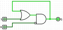
An SR AND-OR latch. Light green means logical '1' and dark green means logical '0'. The latch is currently in hold mode (no change).
From a pedagogy point of view, SR latches drawn as a pair of cantankerous-coupled components (transistors, gates, tubes, etc.) are oft hard to understand for beginners. A didactically easier to empathize fashion is to describe the latch as a unmarried feedback loop instead of the cross-coupling. The following is an SR latch congenital with an AND gate with 1 inverted input and an OR gate. Note that the inverter is not needed for the latch functionality, but rather to make both inputs Loftier-active.
-
SR AND-OR latch performance S R Action 0 0 No change; random initial one 0 Q = ane X 1 Q = 0
Note that the SR AND-OR latch has the do good that S = 1, R = 1 is well divers. In above version of the SR AND-OR latch it gives priority to the R signal over the Due south signal. If priority of S over R is needed, this can exist achieved by connecting output Q to the output of the OR gate instead of the output of the AND gate.
The SR AND-OR latch is easier to understand, because both gates can be explained in isolation. When neither Southward or R is gear up, then both the OR gate and the AND gate are in "hold mode", i.e., their output is the input from the feedback loop. When input South = 1, and so the output of the OR gate becomes 1, regardless of the other input from the feedback loop ("set way"). When input R = i then the output of the AND gate becomes 0, regardless of the other input from the feedback loop ("reset way"). And since the output Q is straight connected to the output of the AND gate, R has priority over S. Latches drawn equally cross-coupled gates may look less intuitive, as the behaviour of one gate appears to exist intertwined with the other gate.
Notation that the SR AND-OR latch tin can be transformed into the SR NOR latch using logic transformations: inverting the output of the OR gate and also the 2nd input of the AND gate and connecting the inverted Q output between these two added inverters; with the AND gate with both inputs inverted being equivalent to a NOR gate co-ordinate to De Morgan's laws.
JK latch [edit]
The JK latch is much less ofttimes used than the JK flip-flop. The JK latch follows the post-obit state tabular array:
-
JK latch truth tabular array J Grand Qnext Annotate 0 0 Q No change 0 1 0 Reset one 0 1 Gear up one 1 Q Toggle
Hence, the JK latch is an SR latch that is made to toggle its output (oscillate betwixt 0 and one) when passed the input combination of xi.[16] Unlike the JK flip-flop, the 11 input combination for the JK latch is not very useful considering there is no clock that directs toggling.[17]
Gated latches and conditional transparency [edit]
Latches are designed to be transparent. That is, input signal changes crusade immediate changes in output. Additional logic can be added to a simple transparent latch to make it non-transparent or opaque when another input (an "enable" input) is not asserted. When several transparent latches follow each other, using the aforementioned enable betoken, signals can propagate through all of them at one time. However, by following a transparent-high latch with a transparent-low (or opaque-high) latch, a master–slave flip-flop is implemented.
Gated SR latch [edit]

NAND Gated SR Latch (Clocked SR flip-flop). Note the inverted inputs.

A gated SR latch circuit diagram constructed from AND gates (on left) and NOR gates (on right).
A synchronous SR latch (sometimes clocked SR flip-bomb) can be made by adding a second level of NAND gates to the inverted SR latch (or a 2nd level of AND gates to the direct SR latch). The extra NAND gates further invert the inputs so SR latch becomes a gated SR latch (and a SR latch would transform into a gated SR latch with inverted enable).
With E high (enable true), the signals can pass through the input gates to the encapsulated latch; all signal combinations except for (0, 0) = hold then immediately reproduce on the (Q, Q) output, i.due east. the latch is transparent.
With E low (enable faux) the latch is airtight (opaque) and remains in the state it was left the concluding time E was high.
The enable input is sometimes a clock signal, but more frequently a read or write strobe. When the enable input is a clock signal, the latch is said to be level-sensitive (to the level of the clock signal), as opposed to border-sensitive similar flip-flops below.
| Symbol for a gated SR latch |

Gated D latch [edit]
This latch exploits the fact that, in the two active input combinations (01 and ten) of a gated SR latch, R is the complement of S. The input NAND phase converts the two D input states (0 and 1) to these two input combinations for the next SR latch by inverting the information input bespeak. The low state of the enable signal produces the inactive "11" combination. Thus a gated D-latch may be considered as a ane-input synchronous SR latch. This configuration prevents application of the restricted input combination. It is also known as transparent latch, data latch, or merely gated latch. It has a data input and an enable signal (sometimes named clock, or control). The discussion transparent comes from the fact that, when the enable input is on, the indicate propagates directly through the excursion, from the input D to the output Q. Gated D-latches are also level-sensitive with respect to the level of the clock or enable signal.
Transparent latches are typically used every bit I/O ports or in asynchronous systems, or in synchronous two-phase systems (synchronous systems that use a two-phase clock), where two latches operating on different clock phases foreclose data transparency as in a master–slave flip-flop.
Latches are available every bit integrated circuits, ordinarily with multiple latches per chip. For example, 74HC75 is a quadruple transparent latch in the 7400 series.
The truth tabular array beneath shows that when the due eastnable/clock input is 0, the D input has no effect on the output. When Eastward/C is high, the output equals D.
| Symbol for a gated D latch |
-

A gated D latch based on an SR NAND latch
-

A gated D latch based on an SR NOR latch
-

An animated gated D latch. Black and white mean logical 'i' and '0', respectively.
- D = 1, E = 1: prepare
- D = i, E = 0: hold
- D = 0, East = 0: agree
- D = 0, E = 1: reset
-

A gated D latch in laissez passer transistor logic, similar to the ones in the CD4042 or the CD74HC75 integrated circuits.
Earle latch [edit]
The classic gated latch designs have some undesirable characteristics.[18] They require double-rail logic or an inverter. The input-to-output propagation may take up to three gate delays. The input-to-output propagation is not constant – some outputs have two gate delays while others take three.
Designers looked for alternatives.[19] A successful alternative is the Earle latch. It requires only a single data input, and its output takes a constant ii gate delays. In addition, the two gate levels of the Earle latch can, in some cases, be merged with the last 2 gate levels of the circuits driving the latch because many common computational circuits take an OR layer followed past an AND layer equally their last two levels. Merging the latch office can implement the latch with no additional gate delays.[18] The merge is unremarkably exploited in the design of pipelined computers, and, in fact, was originally developed by John One thousand. Earle to be used in the IBM System/360 Model 91 for that purpose.[20]
The Earle latch is take chances gratuitous.[21] If the centre NAND gate is omitted, then one gets the polarity hold latch, which is commonly used considering it demands less logic.[21] [22] However, it is susceptible to logic take chances. Intentionally skewing the clock signal can avoid the hazard.[22]
-

Earle latch uses complementary enable inputs: enable active low (E_L) and enable active loftier (E_H)
-

An blithe Earle latch. Blackness and white hateful logical 'one' and '0', respectively.
- D = 1, E_H = 1: set
- D = 0, E_H = i: reset
- D = one, E_H = 0: agree
D flip-flop [edit]

D flip-bomb symbol
The D flip-bomb is widely used. Information technology is also known as a "data" or "delay" flip-bomb.
The D flip-bomb captures the value of the D-input at a definite portion of the clock cycle (such equally the ascent edge of the clock). That captured value becomes the Q output. At other times, the output Q does non change.[23] [24] The D flip-flop tin can be viewed as a memory cell, a naught-order hold, or a delay line.[25]
Truth table:
-
Clock D Qnext Rise edge 0 0 Rise edge 1 i Non-rising X Q
(X denotes a don't care status, pregnant the signal is irrelevant)
Near D-type flip-flops in ICs take the capability to be forced to the prepare or reset land (which ignores the D and clock inputs), much like an SR flip-flop. Usually, the illegal Due south = R = 1 status is resolved in D-type flip-flops. Setting Southward = R = 0 makes the flip-bomb carry as described higher up. Hither is the truth table for the other possible South and R configurations:
-
Inputs Outputs S R D > Q Q 0 ane X X 0 one ane 0 X X 1 0 1 1 X 10 1 1
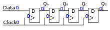
These flip-flops are very useful, equally they class the basis for shift registers, which are an essential role of many electronic devices. The advantage of the D flip-bomb over the D-type "transparent latch" is that the signal on the D input pin is captured the moment the flip-flop is clocked, and subsequent changes on the D input will be ignored until the next clock result. An exception is that some flip-flops have a "reset" signal input, which volition reset Q (to zero), and may be either asynchronous or synchronous with the clock.
The above circuit shifts the contents of the register to the right, i fleck position on each active transition of the clock. The input X is shifted into the leftmost bit position.
Classical positive-edge-triggered D flip-flop [edit]

A positive-border-triggered D flip-bomb

A positive-edge-triggered D flip-flop with set and reset
This circuit[26] consists of two stages implemented by SR NAND latches. The input stage (the two latches on the left) processes the clock and data signals to ensure right input signals for the output stage (the single latch on the right). If the clock is low, both the output signals of the input stage are high regardless of the information input; the output latch is unaffected and it stores the previous state. When the clock signal changes from low to high, only one of the output voltages (depending on the data betoken) goes low and sets/resets the output latch: if D = 0, the lower output becomes low; if D = ane, the upper output becomes low. If the clock signal continues staying high, the outputs proceed their states regardless of the data input and force the output latch to stay in the corresponding state as the input logical zero (of the output stage) remains active while the clock is high. Hence the office of the output latch is to store the data only while the clock is low.
The circuit is closely related to the gated D latch as both the circuits convert the two D input states (0 and 1) to two input combinations (01 and x) for the output SR latch past inverting the data input indicate (both the circuits split the single D betoken in two complementary S and R signals). The difference is that in the gated D latch uncomplicated NAND logical gates are used while in the positive-edge-triggered D flip-bomb SR NAND latches are used for this purpose. The role of these latches is to "lock" the active output producing low voltage (a logical nada); thus the positive-edge-triggered D flip-bomb can also be thought of as a gated D latch with latched input gates.
Principal–slave edge-triggered D flip-flop [edit]

A chief–slave D flip-bomb. Information technology responds on the falling edge of the enable input (usually a clock)

An implementation of a principal–slave D flip-flop that is triggered on the rising edge of the clock
A master–slave D flip-flop is created by connecting two gated D latches in series, and inverting the enable input to one of them. It is chosen principal–slave considering the primary latch controls the slave latch'south output value Q and forces the slave latch to agree its value whenever the slave latch is enabled, every bit the slave latch always copies its new value from the main latch and changes its value only in response to a change in the value of the master latch and clock betoken.
For a positive-edge triggered master–slave D flip-flop, when the clock signal is low (logical 0) the "enable" seen by the first or "master" D latch (the inverted clock signal) is high (logical 1). This allows the "primary" latch to shop the input value when the clock signal transitions from depression to high. As the clock betoken goes high (0 to 1) the inverted "enable" of the commencement latch goes low (1 to 0) and the value seen at the input to the chief latch is "locked". Nearly simultaneously, the twice inverted "enable" of the 2d or "slave" D latch transitions from depression to high (0 to ane) with the clock betoken. This allows the betoken captured at the ascent edge of the clock by the now "locked" primary latch to pass through the "slave" latch. When the clock signal returns to low (1 to 0), the output of the "slave" latch is "locked", and the value seen at the last rising edge of the clock is held while the "master" latch begins to accept new values in preparation for the next rising clock border.
Removing the leftmost inverter in the circuit creates a D-type flip-flop that strobes on the falling edge of a clock signal. This has a truth tabular array like this:
-
D Q > Qside by side 0 10 Falling 0 1 X Falling 1
Dual-edge-triggered D flip-flop [edit]

An implementation of a dual-border-triggered D flip-flop
Flip-Flops that read in a new value on the rising and the falling edge of the clock are called dual-border-triggered flip-flops. Such a flip-flop may be built using two single-edge-triggered D-blazon flip-flops and a multiplexer every bit shown in the image.

Circuit symbol of a dual-edge-triggered D flip-bomb
Border-triggered dynamic D storage element [edit]

A CMOS IC implementation of a dynamic edge-triggered flip-flop with reset
An efficient functional alternative to a D flip-flop can exist made with dynamic circuits (where data is stored in a capacitance) as long every bit it is clocked often plenty; while not a true flip-bomb, it is still chosen a flip-bomb for its functional office. While the master–slave D chemical element is triggered on the edge of a clock, its components are each triggered by clock levels. The "edge-triggered D flip-flop", as it is chosen fifty-fifty though information technology is not a true flip-flop, does not have the master–slave properties.
Edge-triggered D flip-flops are often implemented in integrated high-speed operations using dynamic logic. This ways that the digital output is stored on parasitic device capacitance while the device is not transitioning. This design of dynamic flip flops besides enables simple resetting since the reset functioning tin can be performed by simply discharging 1 or more internal nodes. A common dynamic flip-flop diverseness is the true unmarried-phase clock (TSPC) type which performs the flip-flop operation with lilliputian ability and at high speeds. Even so, dynamic flip-flops volition typically not work at static or low clock speeds: given enough time, leakage paths may discharge the parasitic capacitance enough to cause the flip-flop to enter invalid states.
T flip-flop [edit]

A circuit symbol for a T-type flip-flop
If the T input is high, the T flip-flop changes country ("toggles")[27] whenever the clock input is strobed. If the T input is low, the flip-flop holds the previous value. This beliefs is described by the characteristic equation:
- (expanding the XOR operator)

and can exist described in a truth table:
-
T flip-bomb operation[28] Feature table Excitation tabular array Comment Annotate 0 0 0 Hold state (no clock) 0 0 0 No change 0 1 1 Concord state (no clock) 1 ane 0 No change ane 0 ane Toggle 0 i ane Complement 1 1 0 Toggle 1 0 ane Complement


When T is held loftier, the toggle flip-bomb divides the clock frequency by two; that is, if clock frequency is iv MHz, the output frequency obtained from the flip-flop volition be 2 MHz. This "dissever by" feature has awarding in various types of digital counters. A T flip-flop can likewise be built using a JK flip-bomb (J & Grand pins are connected together and human action as T) or a D flip-flop (T input XOR Qprevious drives the D input).
JK flip-flop [edit]

A circuit symbol for a positive-edge-triggered JK flip-flop
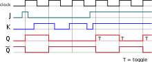
JK flip-flop timing diagram
The JK flip-bomb augments the behavior of the SR flip-bomb (J: Set, K: Reset) by interpreting the J = K = 1 condition as a "flip" or toggle command. Specifically, the combination J = 1, K = 0 is a control to set the flip-flop; the combination J = 0, K = 1 is a command to reset the flip-flop; and the combination J = K = 1 is a command to toggle the flip-flop, i.e., change its output to the logical complement of its current value. Setting J = 1000 = 0 maintains the electric current state. To synthesize a D flip-bomb, only set Yard equal to the complement of J (input J volition act as input D). Similarly, to synthesize a T flip-bomb, set 1000 equal to J. The JK flip-flop is therefore a universal flip-flop, considering it can be configured to piece of work equally an SR flip-flop, a D flip-flop, or a T flip-bomb.
The characteristic equation of the JK flip-flop is:

and the corresponding truth table is:
-
JK flip-flop operation[28] Feature table Excitation table J Thousand Comment Qnext Q Qnext Comment J K 0 0 Hold country Q 0 0 No change 0 10 0 i Reset 0 0 one Gear up 1 Ten 1 0 Set 1 1 0 Reset X i 1 ane Toggle Q 1 1 No change X 0
Timing considerations [edit]
Timing parameters [edit]

Flip-flop setup, hold and clock-to-output timing parameters
The input must be held steady in a flow effectually the rising edge of the clock known as the aperture. Imagine taking a moving-picture show of a frog on a lily-pad.[29] Suppose the frog then jumps into the water. If you lot take a motion picture of the frog as information technology jumps into the h2o, yous will get a blurry film of the frog jumping into the water—information technology's not clear which land the frog was in. But if you lot take a motion picture while the frog sits steadily on the pad (or is steadily in the water), you will go a clear picture. In the same way, the input to a flip-flop must be held steady during the discontinuity of the flip-bomb.
Setup time is the minimum corporeality of time the data input should be held steady before the clock event, so that the data is reliably sampled by the clock.
Hold time is the minimum amount of time the data input should be held steady after the clock event, and then that the data is reliably sampled past the clock.
Aperture is the sum of setup and hold fourth dimension. The data input should be held steady throughout this fourth dimension period.[29]
Recovery fourth dimension is the minimum amount of time the asynchronous gear up or reset input should exist inactive earlier the clock event, then that the data is reliably sampled by the clock. The recovery time for the asynchronous set or reset input is thereby similar to the setup time for the data input.
Removal fourth dimension is the minimum corporeality of fourth dimension the asynchronous set or reset input should exist inactive afterward the clock event, so that the data is reliably sampled past the clock. The removal time for the asynchronous set or reset input is thereby similar to the hold time for the data input.
Curt impulses applied to asynchronous inputs (set, reset) should not exist practical completely within the recovery-removal menses, or else it becomes entirely indeterminable whether the flip-bomb will transition to the appropriate land. In another case, where an asynchronous signal simply makes one transition that happens to fall between the recovery/removal time, somewhen the flip-bomb will transition to the appropriate country, simply a very short glitch may or may not appear on the output, dependent on the synchronous input betoken. This 2nd situation may or may not have significance to a circuit design.
Set and Reset (and other) signals may be either synchronous or asynchronous and therefore may be characterized with either Setup/Concur or Recovery/Removal times, and synchronicity is very dependent on the pattern of the flip-flop.
Differentiation between Setup/Concord and Recovery/Removal times is oftentimes necessary when verifying the timing of larger circuits because asynchronous signals may be constitute to be less disquisitional than synchronous signals. The differentiation offers circuit designers the ability to define the verification conditions for these types of signals independently.
Metastability [edit]
Flip-flops are subject to a problem called metastability, which can happen when two inputs, such as data and clock or clock and reset, are changing at about the same time. When the gild is non clear, within appropriate timing constraints, the issue is that the output may behave unpredictably, taking many times longer than normal to settle to 1 state or the other, or even oscillating several times before settling. Theoretically, the time to settle downwards is not divisional. In a computer system, this metastability can cause corruption of data or a program crash if the state is non stable before another circuit uses its value; in particular, if ii unlike logical paths use the output of a flip-flop, 1 path tin translate it every bit a 0 and the other as a i when it has non resolved to stable state, putting the machine into an inconsistent country.[30]
The metastability in flip-flops tin can be avoided by ensuring that the data and control inputs are held valid and constant for specified periods earlier and after the clock pulse, chosen the setup time (tsu) and the hold time (th) respectively. These times are specified in the data sail for the device, and are typically betwixt a few nanoseconds and a few hundred picoseconds for modern devices. Depending upon the flip-bomb'south internal organization, it is possible to build a device with a zero (or even negative) setup or hold time requirement but not both simultaneously.
Unfortunately, it is non always possible to meet the setup and concur criteria, because the flip-flop may exist connected to a real-fourth dimension betoken that could change at whatsoever time, exterior the control of the designer. In this instance, the best the designer tin can do is to reduce the probability of error to a certain level, depending on the required reliability of the circuit. One technique for suppressing metastability is to connect ii or more than flip-flops in a concatenation, so that the output of each one feeds the data input of the adjacent, and all devices share a common clock. With this method, the probability of a metastable upshot tin be reduced to a negligible value, just never to nil. The probability of metastability gets closer and closer to zero as the number of flip-flops connected in serial is increased. The number of flip-flops being cascaded is referred to as the "ranking"; "dual-ranked" flip flops (ii flip-flops in serial) is a common situation.
So-called metastable-hardened flip-flops are available, which work by reducing the setup and agree times as much as possible, but even these cannot eliminate the problem entirely. This is because metastability is more than merely a thing of circuit pattern. When the transitions in the clock and the data are close together in time, the flip-flop is forced to decide which upshot happened starting time. However fast the device is fabricated, in that location is always the possibility that the input events will be then close together that information technology cannot detect which ane happened first. Information technology is therefore logically impossible to build a perfectly metastable-proof flip-flop. Flip-flops are sometimes characterized for a maximum settling time (the maximum fourth dimension they volition remain metastable under specified weather). In this case, dual-ranked flip-flops that are clocked slower than the maximum allowed metastability time will provide proper conditioning for asynchronous (e.1000., external) signals.
Propagation delay [edit]
Another of import timing value for a flip-flop is the clock-to-output delay (common symbol in data sheets: tCO) or propagation delay (tP), which is the time a flip-bomb takes to alter its output after the clock edge. The time for a high-to-low transition (tPHL) is sometimes dissimilar from the time for a low-to-high transition (tPLH).
When cascading flip-flops which share the same clock (as in a shift annals), it is important to ensure that the tCO of a preceding flip-flop is longer than the hold time (th) of the following flip-bomb, so information nowadays at the input of the succeeding flip-flop is properly "shifted in" post-obit the active edge of the clock. This relationship between tCO and th is commonly guaranteed if the flip-flops are physically identical. Furthermore, for correct functioning, it is easy to verify that the clock menstruation has to be greater than the sum tsu + th.
Generalizations [edit]
Flip-flops can be generalized in at least two ways: past making them one-of-North instead of 1-of-ii, and by adapting them to logic with more than two states. In the special cases of ane-of-3 encoding, or multi-valued ternary logic, such an element may be referred to every bit a flip-flap-bomb.[31]
In a conventional flip-flop, exactly 1 of the ii complementary outputs is loftier. This can be generalized to a retentivity element with Due north outputs, exactly 1 of which is loftier (alternatively, where exactly ane of Due north is depression). The output is therefore always a one-hot (respectively ane-cold) representation. The construction is similar to a conventional cantankerous-coupled flip-flop; each output, when high, inhibits all the other outputs.[32] Alternatively, more or less conventional flip-flops tin be used, one per output, with additional circuitry to make sure only one at a time tin exist true.[33]
Another generalization of the conventional flip-flop is a memory element for multi-valued logic. In this instance the memory element retains exactly 1 of the logic states until the control inputs induce a change.[34] In addition, a multiple-valued clock can besides be used, leading to new possible clock transitions.[35]
See also [edit]
| | Wikimedia Commons has media related to Flip-flops. |
- Latching relay
- Positive feedback
- Pulse transition detector
- Static random-access memory
- Sample and hold, analog latch
References [edit]
- ^ a b Pedroni, Volnei A. (2008). Digital electronics and design with VHDL. Morgan Kaufmann. p. 329. ISBN978-0-12-374270-4.
- ^ a b Latches and Flip Flops (EE 42/100 Lecture 24 from Berkeley) "...Sometimes the terms flip-flop and latch are used interchangeably..."
- ^ a b Roth, Charles H. Jr. "Latches and Flip-Flops." Fundamentals of Logic Design. Boston: PWS, 1995. Print.
- ^ GB 148582, Eccles, William Henry & Jordan, Frank Wilfred, "Improvements in ionic relays", published 1920-08-05
- ^ See:
- Westward. H. Eccles and F. W. Hashemite kingdom of jordan (19 September 1919) "A trigger relay utilizing three-electrode thermionic vacuum tubes," The Electrician, 83 : 298.
- Reprinted in: West. H. Eccles and F. West. Jordan (December 1919) "A trigger relay utilizing 3-electrode thermionic vacuum tubes," The Radio Review, 1 (3) : 143–146.
- Summary in: West. H. Eccles and F. W. Jordan (1919) "A trigger relay utilising three electrode thermionic vacuum tubes," Report of the Eighty-7th Meeting of the British Association for the Advancement of Science: Bournemouth: 1919, September 9–thirteen, pp. 271–272.
- ^ Pugh, Emerson Westward.; Johnson, Lyle R.; Palmer, John H. (1991). IBM'due south 360 and early 370 systems . MIT Press. p. x. ISBN978-0-262-16123-7.
- ^ Flowers, Thomas H. (1983), "The Pattern of Colossus", Register of the History of Computing, 5 (iii): 249, doi:x.1109/MAHC.1983.10079, S2CID 39816473
- ^ Gates, Earl D. (2000-12-01). Introduction to electronics (4th ed.). Delmar Thomson (Cengage) Learning. p. 299. ISBN978-0-7668-1698-five.
- ^ Fogiel, Max; Gu, You-Liang (1998). The Electronics trouble solver, Volume i (revised ed.). Inquiry & Didactics Assoc. p. 1223. ISBN978-0-87891-543-9.
- ^ P. L. Lindley, Aug. 1968, EDN (magazine), (alphabetic character dated June 13, 1968).
- ^ Phister, Montgomery (1958). Logical Pattern of Digital Computers. Wiley. p. 128. ISBN9780608102658.
- ^ US 2850566, Nelson, Eldred C., "High-speed press system", published 1958-09-02, assigned to Hughes Aircraft Co.
- ^ Shiva, Sajjan G. (2000). Estimator blueprint and architecture (3rd ed.). CRC Press. p. 81. ISBN978-0-8247-0368-4.
- ^ Langholz, Gideon; Kandel, Abraham; Mott, Joe L. (1998). Foundations of Digital Logic Pattern. Singapore: World Scientific Publishing Co. Ptc. Ltd. p. 344. ISBN978-981-02-3110-1.
- ^ "Summary of the Types of Flip-bomb Behaviour". Retrieved on 16 April 2018.
- ^ Hinrichsen, Diederich; Pritchard, Anthony J. (2006). Mathematical Systems Theory I: Modelling, State Space Analysis, Stability and Robustness. Springer. pp. 63–64. ISBN9783540264101.
- ^ Farhat, Hassan A. (2004). Digital design and computer system. Vol. i. CRC Press. p. 274. ISBN978-0-8493-1191-8.
- ^ a b Kogge, Peter Thou. (1981). The Compages of Pipelined Computers. McGraw-Hill. pp. 25–27. ISBN0-07-035237-two.
- ^ Cotten, L. W. (1965). "Circuit Implementation of Loftier-Speed Pipeline Systems". AFIPS Proc. Fall Articulation Computer Conference: 489–504. doi:10.1145/1463891.1463945. S2CID 15955626.
- ^ Earle, John G. (March 1965). "Latched Carry-Save Adder". IBM Technical Disclosure Bulletin. 7 (x): 909–910.
- ^ a b Omondi, Amos R. (1999-04-30). The Microarchitecture of Pipelined and Superscalar Computers. Springer. pp. 40–42. ISBN978-0-7923-8463-2.
- ^ a b Kunkel, Steven R.; Smith, James E. (May 1986). "Optimal Pipelining in Supercomputers". ACM SIGARCH Calculator Architecture News. ACM. xiv (two): 404–411 [406]. CiteSeerXx.1.ane.99.2773. doi:10.1145/17356.17403. ISSN 0163-5964. S2CID 2733845.
- ^ The D Flip-Flop
- ^ "Edge-Triggered Flip-flops". Archived from the original on 2013-09-08. Retrieved 2011-12-15 .
- ^ A Survey of Digital Computer Memory Systems
- ^ SN7474 TI datasheet
- ^ "Understanding the T Flip-Flop". oemsecrets.com . Retrieved 29 April 2021.
- ^ a b Mano, 1000. Morris; Kime, Charles R. (2004). Logic and Computer Pattern Fundamentals, 3rd Edition. Upper Saddle River, NJ, Usa: Pearson Pedagogy International. p. 283. ISBN0-13-191165-1.
- ^ a b Harris, South; Harris, D (2016). Digital Design and Reckoner Architecture - ARM Edition. Morgan Kaufmann, Waltham, MA. ISBN978-0-12-800056-4.
- ^ Chaney, Thomas J.; Molnar, Charles E. (April 1973). "Anomalous Behavior of Synchronizer and Czar Circuits". IEEE Transactions on Computers. C-22 (iv): 421–422. doi:10.1109/T-C.1973.223730. ISSN 0018-9340. S2CID 12594672.
- ^ Oftentimes attributed to Don Knuth (1969) (see Midhat J. Gazalé (2000). Number: from Ahmes to Cantor. Princeton Academy Press. p. 57. ISBN978-0-691-00515-seven. ), the term flip-flap-flop actually appeared much before in the computing literature, for instance, Bowdon, Edward Thousand. (1960). The design and awarding of a "flip-flap-bomb" using tunnel diodes (Master's thesis). Academy of Due north Dakota. , and in Alexander, Westward. (Feb 1964). "The ternary estimator". Electronics and Ability. IET. 10 (2): 36–39. doi:10.1049/ep.1964.0037.
- ^ "Ternary "flip-flap-flop"". Archived from the original on 2009-01-05. Retrieved 2009-10-17 .
- ^ US 6975152
- ^ Irving, Thurman A.; Shiva, Sajjan G.; Nagle, H. Troy (March 1976). "Flip-Flops for Multiple-Valued Logic". IEEE Transactions on Computers. C-25 (iii): 237–246. doi:x.1109/TC.1976.5009250. S2CID 34323423.
- ^ Wu, Haomin; Zhuang Nan (1991). "Research into ternary border-triggered JKL flip-flop". Journal of Electronics (China). 8 (Volume eight, Number 3 / July, 1991): 268–275. doi:10.1007/BF02778378. S2CID 61275953.
External links [edit]
- FlipFlop Hierarchy Archived 2015-04-08 at the Wayback Car, shows interactive flipflop circuits.
- The J-Chiliad Flip-Flop

Source: https://en.wikipedia.org/wiki/Flip-flop_%28electronics%29
Posted by: samswortatuslege.blogspot.com
0 Response to "How Many Gated D-latches Are Present In 4 16-bit Registers?"
Post a Comment